 FalconX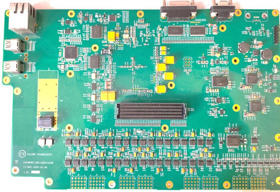
Kintex-7 Customized Development Board
The SP7 Digital Control Card, equipped with the best-in-class performance-per-watt Spartan 7 FPGA, is built for designs requiring sensor fusion such as industrial networking, embedded vision, and automotive applications.
System Overview
The Kintex-7 customized Development Board includes all the basic components of hardware, design tools, IP, and pre-verified reference designs including a targeted design enabling high-performance serial connectivity and advanced memory interfacing.
It supports the SFP communication, 1GBE, Display Port.
Key Capabilities
Kintex-7 FPGA
47K Programmable Logic Cells
High-Speed Memory
DDR3 + Quad-SPI Flash
High-Speed Connectivity
SFP / 1GbE / DisplayPort
Expansion
400-pin FMC HPC
Target Applications
Board Specification
Core mechanical, configuration, memory, communication, I/O, expansion, clocking, and power specifications.
Mechanical
Configuration
Memory
Communication
Control & I/O
Expansion
Clocking & Power
FPGA Resources
Programmable Logic Cells
47K
Block RAM (Kb)
34,380
DSP Slices
1920
Maximum I/O Pins
590
Block Diagram
Reference architecture and system-level connectivity for the Kintex-7 platform.
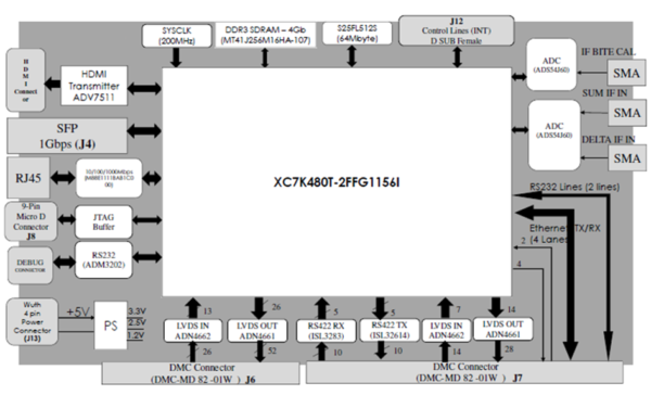
FPGA Processing
Kintex-7 programmable logic provides the processing fabric for high-performance hardware applications.
High-Speed Interfaces
SFP, Gigabit Ethernet, DisplayPort and expansion connectivity support high-speed system integration.
Expansion
A populated 400-pin FMC HPC connector provides a flexible path for system-specific expansion.
System Integration
Designed to integrate hardware, design tools, IP and pre-verified reference designs.
Additional Specifications
Additional specification information reproduced from the FalconX product reference.
Mechanical
Configuration
Memory
RESOURCES
Technical Resources
RESOURCES // FPGA
Kintex-7 Resource Profile
The board reference includes programmable logic, block RAM, DSP resources and a high I/O count intended for demanding hardware development and integration workflows.
Additional Resource Data
The original FalconX page also references a 4-channel data acquisition card based on Zynq-7000 SoC.
4 Channel Data Acquisition Card
Programmable Logic Cells
28K
Block RAM (36 Kb Blocks)
2.1 Mb (545)
DSP Slices
900
Look-Up Tables (LUTs)
17,600
Maximum I/O Pins
PS I/O 128 / PL I/O 125
FALCONX // DEVELOPMENT PLATFORM
Need a customized FPGA development platform?
Talk to the FalconX engineering team about customized development boards, FPGA systems, high-speed interfaces and embedded hardware.